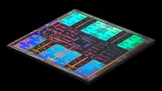
Nvidia has “de-risked” creating GPUs from AMD Zen 2-style multiple chiplets, but its engineers say it’s still not at a point where the technology makes sense in terms of dropping it into a next-gen graphics card design.
Bill Dally, Nvidia’s chief scientist, and Jonah Alben, svp of Nvidia’s GPU engineering, were asked about the growing trend of moving from monolithic to chiplet designs. They explained the company had already done a heap of research into the feasibility of such designs and that “if it became economically the right thing to do” Nvidia would have the technology available to its GPU designers.
It is beginning to look as though the days of the big monolithic processor design, whether CPU or GPU, are numbered. Much like the days of processor past, where the beefy single core designs gave way to more lithe multi-core CPUs, the sorts of massive, transistor-heavy chips that have dominated the computing world are increasingly giving way to silicon packages mixing multiple smaller chiplets. The latest AMD Zen 2 design is the most obvious, and commercially ready, example of this where the processing cores exist on separate chiplets to the I/O die.
This has been done for a few reasons, but the economic one is arguably the most tangible. With the latest Ryzen design AMD has moved to the most advanced production node around – TSMC’s 7nm – and with new processes come increased expense and lower production yields. AMD has gotten around this by using the chiplet design to create smaller individual slices of silicon than would otherwise be needed for a large monolithic CPU, which are both cheaper to manufacturer and offer better yields too.
Then for the bigger, non-performance sensitive I/O die it has stuck with a 14nm lithography that was cheaper still and wouldn’t directly benefit from being built on the most advanced node.
Intel is also looking at different, chiplet-style packaging techniques for its CPUs, taking the EMIB connection for discrete silicon, first used in the AMD/Intel joint Kaby Lake G effort, and the Foveros stacking technique to create modular chips with vertical and horizontal interconnectivity.
Nvidia isn’t one to be left out of a good ol’ fashioned advanced technology race and so has been investigating chiplet-style technologies for many years. In an interview with SemiconductorEngineering Dally explains how, with its Volta and Pascal GPUs, Nvidia has already demonstrated jamming discrete chips together on a silicon interposer, though that’s just a GPU and some high bandwidth memory.
But it has also demonstrated a 16nm, 32-module GPU prototype for deep learning that uses multiple discrete chips, with 16 ‘processing elements’ in each, all working together on GPU workloads.
“This gives us a bunch of technologies on the shelf that at some point in time,” says Dally, “if it became economically the right thing to do to, assemble GPUs from multiple chiplets, we basically have de-risked the technology. Now it’s a tool in the toolbox for a GPU designer.”
The interviewer then asked where the crossover point is with the industry moving down to 7nm and then onto 5nm… where is the crossover point for GPU chiplets to actually become worthwhile? To which Alben replied, “We haven’t hit it yet.”
But when it comes to gaming GPUs I’m not convinced we ever will. With CPUs it’s a lot easier to combine multiple chips together to work for a common processor-y goal on their specific workloads. And for GPUs simply chewing through large datasets or deep learning the hell out of something it’s a doddle too, but when your GeForce graphics card is trying to spit out multiple game frames rendered on multiple chiplets it’s a whole lot tougher.
CrossFire and SLI haven’t died for nothing, you know…
