Abstract
Nanochanneled silicon targets with high positron/positronium (Ps) conversion rate and efficient Ps cooling were produced. Morphological parameters of the nanochannels, such as their diameter and length, were adjusted to get a large fraction of thermalized Ps at room temperature being emitted into vacuum. Ps cooling measurements were conducted combining single-shot positron annihilation lifetime spectroscopy and Doppler spectroscopy of the 13S → 23P transition. 2γ–3γ annihilation ratio measurements were also performed to estimate the positron/Ps conversion efficiency. In a converter with nanochannel diameter of 7–10 nm and depth of 3.89 μm, ∼28% of implanted positrons with an energy of 3.3 keV was found to be emitted as Ps with a transverse kinetic energy of 11 ± 2 meV. The reduction of the nanochannels depth to 1.13 μm, without changing the nanochannel diameter, was found to result in a less efficient cooling, highlighting the presence of Ps reflection from the bottom end of nanochannels.
Original content from this work may be used under the terms of the Creative Commons Attribution 4.0 licence. Any further distribution of this work must maintain attribution to the author(s) and the title of the work, journal citation and DOI.
1. Introduction
Positronium (Ps), the bound state of an electron and its antiparticle, the positron (e+) [1], is the lightest purely leptonic matter/antimatter atom. Its long-lived ground state, the 13S state ortho-positronium, o-Ps, has a lifetime of 142 ns in vacuum and predominantly annihilates into three gamma rays (3γ). The short-lived 11S ground state para-positronium, p-Ps, has a lifetime in vacuum of only 125 ps and its annihilation occurs via 2γ emission (as for direct positron–electron annihilation). Production and emission into vacuum of a large amount of Ps with kinetic energies smaller than a few tens of electronvolts is of great interest for several fundamental experiments. These include tests of quantum electrodynamics (QED) [2] and matter/antimatter symmetries [3], probing of gravitational force on Ps atoms excited to metastable levels [4–8] and production of anti-hydrogen by charge exchange reaction [9–11].
In recent years, efficient sources of Ps have been synthesized by exploiting either silica-based disordered porous systems [12–14] or oxidized nanochanneled silicon targets [15, 16]. Indeed, Ps is known to be formed in SiO2 irradiated with positrons since 1968 [17]. Subsequent studies have shown that Ps formation in SiO2 occurs both via surface and bulk processes [18–20] with an overall e+/Ps conversion efficiency up to 84% of the implanted e+ [21]. Both processes typically result in Ps atoms emitted into the vacuum with energy of the order of ≈eV [20]. Emission of colder Ps into the vacuum can be obtained by introducing porous structures in the SiO2 matrix. In these systems, Ps is firstly emitted into the pores. While 11S Ps annihilates in a short time, 13S Ps, thanks to its relatively long lifetime, can cool (i.e. lose a fraction of its energy) by collisions [22, 23] with the inner surfaces of the porous SiO2 material, eventually diffuse along the pore network and be emitted into the vacuum with a significantly lower energy [13, 16, 23–26]. The Ps emission energy into the vacuum depends on the number of collisions with the walls and the energy-loss rate per collision that is determined by the characteristics of the surface of the pores [13, 16, 23–27]. The number of collisions is decided by the depth at which Ps is formed and by the morphology of the pores (namely shape, length, diameter, interconnection and tortuosity) [13, 16, 23–26, 28]. In large pores, the rate of interaction with the inner surfaces is reduced and the cooling time required to reach a given temperature is consequently extended [27, 29]. While in small pores, quantum confinement sets a lowest energy threshold Ps cannot go below [13, 30]. The result is that the average kinetic energy of Ps emitted by SiO2 porous e+/Ps converters is usually higher than the thermal energy of the target [13, 16, 23–26].
Oxidized nanochanneled silicon e+/Ps converters have been introduced in 2010 [15, 16]. These converters offer the possibility to tune the nanochannel diameter and length by acting on the synthesis parameters [15, 31]. The nanochannel orientation can be changed by choosing the silicon crystal orientation [32] and the depth of Ps formation by the positron implantation energy [15, 16]. However, even if the physical parameters that contribute to the cooling of Ps are known, it is difficult to match them to optimize the fraction of emitted Ps with an energy at thermal equilibrium with the medium. Targets with nanochannels of 5–8 nm diameter etched in silicon p-type (100) with resistivity of 0.15–0.21 Ω cm were investigated with 2γ–3γ annihilation ratio measurements (in some works also referred as peak-to-valley measurements) and Ps time of flight measurements [16]. Around 35% of e+ implanted at a mean depth ⟨z⟩ ∼ 190 nm in the converter at room temperature (RT) were found to be emitted as Ps with an average one-directional kinetic energy perpendicular to the surface of ∼140 meV [16]. Slower Ps with one-directional kinetic energy of ∼96 meV has been observed in the same converters after e+ implantation at ⟨z⟩ ∼ 470 nm (7 keV e+ implantation energy). In this case, the emitted Ps amounted to 25% of the implanted e+ [16]. The decrease in the average emission energy has been attributed to the increase in the number of collisions before the emission [16]. Also as, in each collision, the e+ of Ps can annihilate with an electron of the walls (pick-off annihilation), the reduction in the fraction of emitted Ps is ascribable to higher number of interactions. Only a small fraction (5% of implanted positrons) was found to be emitted with thermal energy at RT from these converters.
Converters with larger nanochannels of 10–13 nm in diameter have been synthetized from silicon p-type (111) with resistivity 0.1–1.5 Ω cm. The choice of larger nanochannels was motivated by the intention to overcome quantum confinement limitations [13, 30]. Silicon with orientation (111) instead of (100) has been chosen because in the former case nanochannels are expected to form a network at 45° with respect to the surface while in the second case they are expected to be rather perpendicular to the surface [32]. Thus, Ps formed at the same depth has to travel a longer path in Si (111) than in Si (100) converters to reach the surface experiencing a higher number of interactions with the pore walls. Therefore, this choice allows a high emitted Ps fraction to be maintained with low emission energy by lowering the positron implantation energy (i.e. using positrons with a narrower implantation profile [33]). These last converters were used to produce Ps in vacuum for experiments of Ps laser excitation to metastable levels [34–38]. Doppler broadening spectroscopy of the laser-excited 13S → 33P transition [34] and time of flight measurements of Ps in 23S state [36] have shown that Ps addressed 20 ns after e+ implantation at ⟨z⟩ ∼ 140 nm (3.3 keV e+ implantation energy) in the converter at RT has an average one-directional kinetic energy of ∼60 meV.
In the present work we show how performances of the converters can be drastically improved by etching nanochannels of 7–10 nm of diameter in silicon p-type (111) with resistivity of 0.1–1.5 Ω cm, and implanting e+ at a mean depth of ⟨z⟩ ∼ 140 nm (3.3 keV e+ implantation energy). The transverse kinetic energy of Ps emitted from these e+/Ps converters kept at RT was measured via Doppler broadening spectroscopy of the laser-induced 13S → 23P transition. Single-shot positron annihilation lifetime spectroscopy (SSPALS) [39, 40] was used to quantify the amount of laser-excited Ps. The absolute e+/Ps conversion and emission efficiencies into the vacuum were estimated by 2γ–3γ annihilation ratio measurements [41]. Our data indicate that a large quantity (∼28% of the implanted e+) of Ps emitted from a target with a nanochanneled region ∼3.89 μm deep had a transverse kinetic energy of 11 ± 2 meV, corresponding to the thermal energy in one-dimension. An incomplete thermalization was observed in a converter with a less deep nanochanneled region.
2. Experimental methods
2.1. e+/Ps converters
Positron/positronium converters were synthetized starting from substrates of silicon p-type (111) with resistivity 0.1–1.5 Ω cm. Nanochannels were produced via electrochemical etching. The etching solution was realized by adding absolute ethanol to a commercial aqueous solution at 48% of HF with a volume ratio of 1:3 = HF: ethanol. An etching current of 10 mA cm−2 was used. After the electrochemical etching, the samples were cleaned in absolute ethanol ⩾99.8% and oxidized in air at 100 °C for 2 h. As shown in reference [15], a fine tuning of the nanochannel diameter can be obtained by different number of etchings in HF etching solution for 1 min and re-oxidation in air at 100 °C for 2 h. In the present work, we produced two targets subject to a single cycle of re-etching and re-oxidation (named #1 in reference [15]). The nanochannel length is determined by the anodization duration [31]. A first target was synthetized with an anodization time of 10 min (hereafter labelled #1a) and a second one with a time of 4 min (#1b in the following).
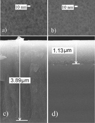
The diameter of the nanochannels and the thickness of the nanochanneled region were evaluated by scanning electron microscopy (SEM) carried out by a high resolution JEOL JSM-7001F thermal field emission SEM. Accelerating voltage ranges from 0.5 to 30 kV and its resolution is 1.2 nm at 30 kV. SEM pictures of the surface of the two targets are reported in figures 1(a) and (b) while the pictures of their sections are reported in figures 1(c) and (d).
Figure 1. SEM pictures of the surface of samples #1a and #1b are reported in (a) and (b), respectively. SEM pictures of the section of samples #1a and #1b are shown in (c) and (d), respectively. The thickness of the nanochanneled region is given for both the targets.
Download figure:
Standard image High-resolution imageAccording to the SEM pictures of the surfaces of the converters, the nanochannel diameter ranges between 7 and 10 nm in both targets. The percentage of the surface not covered by nanochannels amounts to ∼80% of the overall while ∼20% of the surface is etched. This allows us to estimate the density of the nanochanneled region to be around 1.9 g cm−3 (=2.33 g cm−3 (density of silicon) × 0.8, see also reference [15]) in both the targets. The SEM pictures of the sections of the converters indicate that the thickness of the nanochanneled region is ∼3.89 μm for sample #1a and ∼1.13 μm for #1b. By comparison with converters synthetized from silicon p-type (100) with resistivity of 0.15–0.21 Ω cm, the nanochanneled region in the present converters is about two times deeper for a comparable anodization time [15]. Several characteristics of the substrate (among them crystal orientation, range of resistivity, feature of the wafer surface, sample size) could be at the origin of the observed difference in the etch rate [42].
2.2. 2γ–3γ annihilation ratio measurements
The efficiencies of e+/Ps conversion and emission into the vacuum of the two converters were estimated via 2γ–3γ annihilation ratio measurements. Measurements were performed with the Trento positron beam [43] by scanning the fraction of implanted e+ annihilating into 3γ, F3γ
(E), as a function of the positron implantation energy, E. The term E is related to the mean positron implantation depth, ⟨z⟩, through the equation  , where ρ is the material density [33]. The scan was carried out changing the positron implantation energy from 1 to 21 keV. The gamma rays generated by direct e+ annihilations and Ps annihilations were detected by a high purity germanium detector (HPGe) at a distance of about 3.5 cm from the samples. The HPGe detector had 45% efficiency and 1.4 keV energy resolution at 511 keV [41, 44]. The term F3γ
(E) was calculated as the ratio of the 2γ annihilations in the 511 keV annihilation peak and the 3γ annihilations in the region between 410 and 500 keV [41] after calibration with a Ge crystal held at 1000 K to have 0% and 100% Ps formation in the present experimental conditions [41, 45]. The error on F3γ
(E), both due to 0% and 100% evaluation, was estimated to be less than 3.5% [15, 45]. Further details about the measurement system and the technique are given elsewhere [15].
In order to guarantee a constant Ps production, the converters were thermally treated in situ, in ultra-high vacuum at 100 °C for 30' to remove eventual contaminants before the measurements [38, 46].
2.3. Ps kinetic energy measurements: SSPALS measurements and Ps laser excitation
The transverse kinetic energy of the Ps emitted by the converters was probed by exploiting the Doppler broadening of the Lyman-α resonance. The measurement was performed as follows. Bursts containing ∼107 e+ were prepared using the AEgIS e+-system at CERN and implanted into the converters with an energy of 3.3 keV. Briefly, e+ were produced by a 22Na source, slowed by a solid Ne moderator [47] to a kinetic energy of a few eV, trapped and cooled in a Surko-style trap through the use of buffer gas [48]. Subsequently, e+ were moved to a second trap (accumulator) where the positron plasma containing ∼107 e+ was stored and then extracted by fast pulsing the electric potential on the trap electrodes in the form of 20 ns bunches. The positron cloud was then magnetically transported in the direction of a chamber dedicated to Ps experiments. Here positrons were further compressed to about 7 ns in time (FWHM) using a 24-electrode buncher [49, 50] and implanted onto the converter with the final kinetic energy of 3.3 keV (see references [34, 35, 50] for details). The positron spot was of ∼3 mm in diameter [50]. In the present measurements, the target was kept at RT.
The time distribution of γ rays emitted by e+ and Ps annihilations (SSPALS-spectrum [39, 40]), was acquired with the same procedure used in references [34, 35]. A 20 × 25 × 25 mm PbWO4 scintillator, coupled to a Hamamatsu R11265-100 photomultiplier tube and digitized by an HD4096 Teledyne LeCroy oscilloscope, was placed 40 mm above the target.
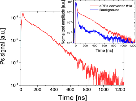
An example of two SSPALS spectra, one measured in the absence of Ps formation (by implantation of e+ on the surface of a microchannel plate, MCP, placed in the experimental chamber [50]) and one in the presence of Ps formation (by implantation of e+ into the converter #1a), is shown in the inset of figure 2. In the absence of Ps formation, SSPALS spectra present a prompt peak, given by the fast 2γ annihilations of e+ implanted in the target. On the right side of the peak, the signal quickly decreases and reaches the noise level in less than 100 ns. The small structures in the spectrum at longer times are photomultiplier ion after pulses [39, 40]. In the presence of Ps formation, SSPALS spectra show a long tail on the right side of the prompt peak. Such a tail is dominated by the 3γ decays of Ps emitted into vacuum. The Ps signal is the difference between the two spectra normalized to the peak height (see main panel in figure 2).
Figure 2. The difference between two SSPALS spectra (Ps signal) measured in a target with Ps formation (e+/Ps converter #1a) and on the surface of the MCP without Ps formation (background) is reported in the main panel. The two SSPALS spectra, normalized to the peak height, are shown in the inset (converter #1a in red and background in blue). Positrons were implanted with energy of 3.3 keV. Each reported SSPALS spectrum is the average of 40 single shots.
Download figure:
Standard image High-resolution imageVacuum-emitted Ps atoms were probed by photo-excitation and photo-ionization, by introducing two laser pulses: an ultra-violet (UV) at 243 nm and a visible (VIS) at 532 nm. The UV drives the 13S → 23P transition and the VIS immediately photo-ionizes the excited fraction. The broadband 243 nm pulse was produced by frequency doubling a broadband 486 nm pulse in a barium borate crystal, produced by a commercial Continuum ND4600 amplified dye laser. The dye oscillator cavity and amplifier were operated with a mixture of Coumarin 480 and Coumarin 500 dissolved in ethanol in optimal proportions (50 ml of Coumarin 500 (2 g l−1) + 150 ml of Coumarin 480 (1 g l−1) + 300 ml ethanol for the oscillator, 20 ml Coumarin 500 (2 g l−1) + 80 ml Coumarin 480 (1 g l−1) + 450 ml ethanol for the amplifier), as described in details in reference [51]. The dye system was pumped by a frequency-tripled commercial 1064 nm CNI Model LPS-L-532 Q-switched ND:YAG pump, routinely producing 355 nm laser pulses of 10 ns temporal FWHM and 100 mJ energy, pumping the dye laser. The 243 nm peak energy was ∼900 μJ with fresh dye solutions and maximum pump power. The UV beam, with an astigmatic Gaussian spatial profile of 1.0 × 2.0 mm FWHM (∼1.8 × 3.7 mm full width at tenth of maximum, FWTM) in the horizontal and vertical directions respectively and with a Gaussian temporal profile of 8 ns FWHM. The bandwidth of the 243 nm pulses was 50 GHz. The intense 532 nm pulses were produced by frequency doubling the first harmonic of an EKSPLA NL303-HT laser pump in a KDP crystal, producing up to 65 mJ of 532 nm in a circular, top-hat spatial profile beam of ∼12 mm FWHM with a Gaussian temporal profile of 4 ns FWHM. The use of two independent laser pumps allowed the pulses to be independently triggered and tuned with a 1 ns resolution. The mutual jittering between the two laser pulses was measured to be <2 ns in a typical experimental run. Both laser beams were aligned grazing the surface of the e+/Ps converter.
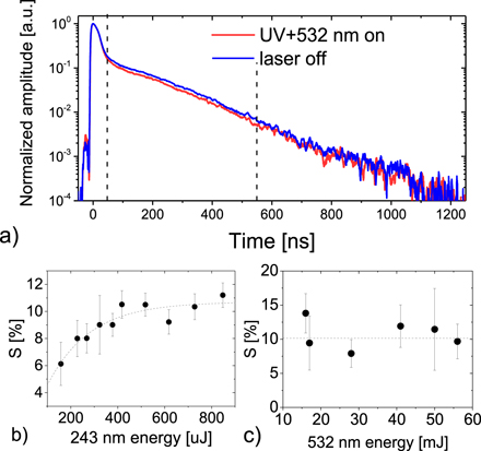
The 13S → 23P laser excitation and photoionization results in a decrease of the Ps population decaying via three gammas. An example is reported in figure 3(a) where SSPALS spectra of Ps emitted into vacuum by target #1a with laser off and UV + VIS lasers on are shown. In this measurement, the UV wavelength was set on resonance at λ0 = 243.01 nm (in vacuum) and both lasers were shot with a delay of 10 ns from the positron implantation. Each reported SSPALS spectrum is the average of 40 single shots. The change in the Ps population induced by the interaction with the two laser pulses was quantified by using the S parameter evaluated as:

where foff and fon are the averages of the normalized areas foff-i and fon-i below the ith SSPALS shot, calculated between 50 and 550 ns from the prompt peak with lasers off and on, respectively [35–37].
Figure 3. (a) SSPALS spectra of Ps (emitted into vacuum by converter #1a) with laser off in blue and UV + VIS lasers on (243.01 nm + 532 nm) in red. The UV energy was 700 μJ while VIS energy was 50 mJ. Each spectrum is the average of 40 single shots. The vertical dashed lines mark the area between 50 and 550 ns from the prompt peak used to evaluate the S parameter. S parameter vs UV energy (with VIS energy set at 50 mJ) are shown in panel (b) and VIS energy (with UV energy set at 500 μJ) in panel (c). The dashed lines are guide for the eye.
Download figure:
Standard image High-resolution imageThe saturation laser energy of both 13S → 23P and 23P → ionization transitions was studied by measuring the S parameter as a function of the UV and VIS energy, respectively (see figures 3(b) and(c)). Also these measurements were performed on sample #1a. The measurements show that 243 nm laser is in saturation for energy above ∼500 μJ while the 532 nm laser saturates above ∼15 mJ.
The Doppler broadening of the Lyman-α resonance of Ps was studied by acquiring the S parameter as a function of the UV laser wavelength [13, 52, 53]. The wavelength of the UV pulse (λ) was varied around the resonance between 242.7 and 243.2 nm. Doppler broadening experiments were conducted keeping the energy of the UV laser pulse around 700 μJ and the VIS energy around 50 mJ to guarantee the saturation of the 13S → 23P and 23P → ionization transition, respectively.
3. Results and discussion
3.1. Estimation of Ps amount emitted into vacuum
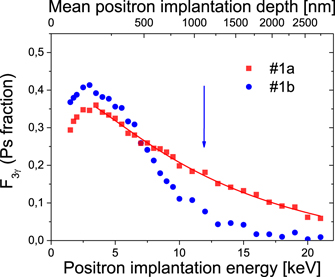
The fraction F3γ (E) of implanted positrons annihilating via 3γ vs positron implantation energy E is shown in figure 4 for both the studied converters. The corresponding mean positron implantation depth in the converters, assuming the density ρ = 1.9 g cm−3, is shown as the upper abscissa. In both targets, F3γ (E) tops out at E ∼ 3–3.5 keV. The maximum value is ∼0.35 and ∼0.41, in #1a and #1b, respectively.
Figure 4. Fraction of implanted e+ annihilating via 3γ, F3γ , vs positron implantation energy E for the converter #1a (red squares) and #1b (blue circle). The vertical arrow marks the upper boundary of the nanochannelled region of #1b. The one of #1a is out of the scale (see figure 1). The continuous line through the points of #1a is the best fit obtained by the diffusion model described in reference [15] (see text).
Download figure:
Standard image High-resolution imageThe slight decrease of F3γ (E) observed at E lower than 2–3 keV is attributable to both the presence of a lower Ps formation at low positron implantation energies [54] and Ps escaping from the nanochannels after only few collisions with walls and hence with a higher kinetic energy. These Ps atoms can annihilate far-away from the HPGe detector and be detected with a reduced efficiency (see reference [15] for a more detailed explanation).
At positron implantation energy higher than 3–3.5 keV, F3γ (E) shows a progressive decrease that is steeper in #1b than in #1a. The observed decrease is due to the presence of two contributions: (i) at high E, the fraction of Ps able to escape from the nanochannels is reduced by the 2γ pick-off annihilations of Ps with an electron of the nanochannel walls and (ii) at high E, a fraction of implanted e+ annihilates in the unetched Si bulk where Ps formation does not occur. The weight of the two contributions is determined by the Ps diffusion length in the nanochannels and by the thickness of the nanochanneled region.
In order to extract the Ps diffusion length in the nanochannels and the fraction of Ps emitted into the vacuum, the F3γ (E) curve measured in #1a was fitted above E = 3.5 keV with the diffusion model described in reference [15]. The fit was performed on the converter with the thicker nanochanneled region because the model assumes nanochannels with infinite length and it does not consider the decrease of Ps formation with the implantation depth due to the effect (ii). The best fit (continuous line in figure 4) points out that the diffusion length in the nanochannels of #1a is 1200 ± 200 nm. This diffusion length is around 50% longer than the one observed in nanochannels of similar diameter but synthetized in Si p-type (100) with resistivity of 0.15–0.21 Ω cm [15]. The found diffusion length is well shorter than the thickness of the nanochanneled region in #1a, while it is longer than that in the nanochannels of #1b. This confirms the expectation that in #1a the effect (i) is predominant, while in #1b the implantation of e+ in the Si bulk is significant and makes the decrease of F3γ (E) steeper than in #1a. Moreover, the fit indicates that the contribution to F3γ given by Ps annihilating via 3γ inside the pores is negligible [15]. Thus, the observed F3γ signal at each E is almost entirely given by Ps back diffused to the surface and emitted into the vacuum. As the nanochannels diameter is found to be identical in the two targets (figure 1) and the interconnectivity of the channel is expected to be the same due to the production procedure, also the F3γ signal measured in #1b is expected to be dominated by Ps emitted into vacuum.
Consequently, the higher F3γ signal observed in #1b than in #1a at E ∼ 3–3.5 keV could be ascribed to the different nanochannel length and to the reflection from the nanochannel bottom end [55] that in the thinner #1b target can result in a more abundant emission into the vacuum.
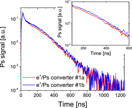
SSPALS measurements confirm that Ps production given by converter #1b is slightly larger than the one by #1a in the proximity of their F3γ (E) maximum (the spectra were acquired at E = 3.3 keV, ⟨z⟩ ∼ 140 nm). Ps signals in each converter, estimated as difference of SSPALS curves with Ps formation and the background without Ps formation, are shown in figure 5. By comparing the areas between 0 and 1200 ns below the two curves, the Ps signal measured in #1b results ∼16% larger than the one observed in #1a. The observed difference is in agreement with the one indicated by the F3γ (E) measurements.
Figure 5. Ps signal estimated as difference of SSPALS for a target with Ps formation and the MCP without Ps formation. Ps signals for e+/Ps converter #1a (red curve) and #1b (blue curve) are reported. A detail is shown in the inset.
Download figure:
Standard image High-resolution image3.2. Ps mean velocity evaluation
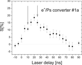
In order to find the time at which the largest fraction of Ps is laser excited, a scan of the S parameter as a function of the delay of the two synchronized lasers (UV wavelength set on resonance) with respect to the positron implantation instant was performed. The curve measured for converter #1a is reported in figure 6.
Figure 6. S-parameter as a function of the UV + 532 nm laser delay with UV laser on resonance. The measurement was performed on converter #1a. The vertical arrows mark the time delay where the 13S → 23P transition line shapes for Ps emitted from the two converters were measured (see text).
Download figure:
Standard image High-resolution imageThe vertical arrows in figure 6 mark the delays at which the transverse kinetic energy of the emitted Ps was measured (10 ns and 25 ns of delay, respectively). The two delay times have been chosen to sample the velocity of emitted Ps in the proximity of the time at which the maximum Ps laser excitation occurs (around 20 ns).
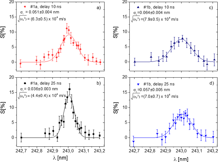
The scan of S parameter as a function of the UV laser wavelength, performed following the procedure reported in section 2.3, is shown in figure 7. Each S value was calculated according to equation (1) from a set of 80 SSPALS single-shot spectra (40 with lasers on and 40 with lasers off acquired in alternated mode). The line shapes of the 13S → 23P transition, measured in #1a at 10 ns and 25 ns, are reported in figures 7(a) and (b), respectively. The measurements performed in #1b at 10 ns and 25 ns are shown in figures 7(c) and (d), respectively. As the width of the 13S → 23P transition is dominated by Doppler broadening, it can be used to obtain the Ps velocity in the direction of the UV laser. The experimental data are fitted to:

where σλ
is the Gaussian width. The root mean square (RMS) velocity along the laser propagation axis x,  , can be calculated as
  while the mean transverse kinetic energy is
  , where c is the speed of light and mPs the mass of Ps [53].
Figure 7. 13S → 23P transition line shapes for Ps emitted from different converters and with different delays between the e+ implantation and the laser shot. The transition lines measured in #1a at 10 ns and 25 ns of laser delay are shown in (a) and (b), respectively. Transition lines measured in the converter #1b at 10 ns and 25 ns of laser delay in (c) and (d), respectively. The measurements were performed by implanting positrons with an energy of 3.3 keV ( ∼ 140 nm). The solid lines are Gaussian fits. The sigma corresponding to each transition line and the relative RMS Ps velocity is reported (see text).
Download figure:
Standard image High-resolution imageThe RMS Ps velocities (mean Ps energies) obtained from the Doppler profiles measured in #1a are (6.3 ± 0.5) × 104 m s−1 (22 ± 4 meV) for a laser delay of 10 ns and (4.4 ± 0.4) × 104 m s−1 (11 ± 2 meV) for a delay of 25 ns. The kinetic energy measured at 25 ns corresponds to the complete thermalization of Ps in the direction of the laser in the target kept at RT. The different velocities at different laser delays can be explained with the fact that the UV laser pulse, thanks to its brief duration and its limited spatial dimension, excites only the fraction of the emitted Ps in front of the target at the time when the laser is shot [36]. Thus, the most delayed laser pulse addresses Ps that resided longer in the nanochannels losing more energy by collision with the walls. The RMS Ps velocities (mean Ps energies) measured in #1b are higher than the ones in #1a: (7.9 ± 0.5) × 104 m s−1 (35 ± 5 meV) for a delay of 10 ns and (7.0 ± 0.7) × 104 m s−1 (28 ± 6 meV) for 25 ns. This increase of the velocities (energies) could arise from the previously mentioned Ps reflection from the nanochannel bottom end that could induce a slightly shorter permanence time of Ps inside target #1b compared to in #1a with a consequent less efficient cooling.
The fitted S value of the 13S → 23P peak at resonance (figure 7) is 10.4 ± 0.8 and 13.9 ± 1.0 for converter #1a at 10 and 25 ns, respectively. In #1b, it is 7.5 ± 0.4 and 7.8 ± 0.4 at 10 and 25 ns, respectively (see table 1). These values can be roughly approximated as the following product:

where d is the excitation efficiency imposed by the bandwidth coverage of the UV laser, s the saturation efficiency of the 13S → 23P → ionization process, η is the laser coverage of the solid angle of the Ps cloud and ɛ is the fraction of Ps within the measured velocity range.
Table 1. S value at resonance and average velocity of Ps measured at 10 and 25 ns of lasers delay in converter #1a and #1b. The angle of the spherical wedge, θ, excitable with the UV laser bandwidth (∼50 GHz) and the corresponding excitation efficiency, d, are also reported (see text).
| Converter | Delay time (ns) | S (%) at resonance | Average velocity (104 m s−1) | Wedge angle (θ) | Excitation efficiency (d) |
|---|---|---|---|---|---|
| #1a | 10 | 10.4 ± 0.8 | ∼6.3 | ±12° | ∼0.133 |
| 25 | 13.9 ± 1.0 | ∼4.4 | ±16° | ∼0.177 | |
| #1b | 10 | 7.5 ± 0.4 | ∼7.9 | ±9.5° | ∼0.106 |
| 25 | 7.8 ± 0.4 | ∼7.0 | ±10.5° | ∼0.117 |
The UV pulse, due to its bandwidth of ∼50 GHz, selectively excites only the emitted Ps with a velocity component parallel to the laser propagation axis, vx,BW
, with |vx,BW| < 1.3 × 10⁴ m s−1. Thus, only Ps expanding within a spherical wedge, whose angle is determined by the Ps average velocity, is addressable (see also references [8, 35]). The wedge angles calculated as  for the different experimental conditions are reported in table 1. From previous measurements, Ps emission is expected to be essentially isotropic in velocity [34, 36, 38]. A further evidence of the isotropy of the Ps velocity comes from the S scan of figure 6 where the excitation signal in #1a disappears after around 70 ns from the positron implantation. As Ps has to travel around 3–4 mm to cross the UV laser spot (see UV FWTM given in section 2.3), the velocity needed to cover this space within 70 ns is ∼4.2–5.7 × 10⁴ m s−1, in good agreement with the measured transverse velocity in this target. In the light of the Ps velocity isotropy, the fractions of Ps expanding within the spherical wedges with the reported angles can be approximated as
  . The values of d for the two converters for both delay times are reported in table 1.
Taking into account the energy of the UV and VIS laser pulses used in the present scan and according to the observation of the saturation of both UV and VIS energies shown in figures 3(b) and (c), the term s gets closer to 1. Given the dimensions of the laser and the e+ beam and the alignment of the laser grazing the target, the laser coverage of the solid angle of the Ps cloud, η, is expected to be not far from unity. If one assumes s and η = 1, equation (3) can be simplified to ![$S\left[\%\right]=100\%\;\;{\ast}\;\;d\;\;{\ast}\;\;\varepsilon $](https://content.cld.iop.org/journals/0953-4075/54/8/085004/revision3/babf6b6ieqn8.gif) and a lower bound for the fraction of Ps within each measured velocity range, ε, can be roughly estimated from the fitted s values and the geometrical evaluations of d (table 1). We find that the fraction of Ps with average velocity of ∼4.4 × 10⁴ m s−1 (measured in #1a at 25 ns) is, at least, ɛ ∼ 0.8 of the entire emitted Ps. As the emitted Ps from this target is around 35% of the implanted e+ at 3.3 keV (from fit of figure 4), ∼28% (=35% × 0.8) of e+ implanted in the converter #1a kept at RT is emitted as completely thermalized Ps. Similarly, the fraction of Ps with average velocity of ∼6.3 × 10⁴ m s−1 (measured in #1a at 10 ns) is, at least, ɛ ∼ 0.8 of the entire emitted Ps. The fact that ɛ ∼ 0.8 in the two cases means that, in the time elapsed between 10 ns and 25 ns, there is a balance between the fast Ps fraction escaping from the laser spot and the fraction, with lower velocity, that enters the laser spot after delayed emission from the target. For sample #1b, we find that at least ɛ ∼ 0.7 and ∼0.65 are emitted with an average velocity of ∼7.9 × 10⁴ m s−1 and ∼7.0 × 10⁴ m s−1, respectively.
and a lower bound for the fraction of Ps within each measured velocity range, ε, can be roughly estimated from the fitted s values and the geometrical evaluations of d (table 1). We find that the fraction of Ps with average velocity of ∼4.4 × 10⁴ m s−1 (measured in #1a at 25 ns) is, at least, ɛ ∼ 0.8 of the entire emitted Ps. As the emitted Ps from this target is around 35% of the implanted e+ at 3.3 keV (from fit of figure 4), ∼28% (=35% × 0.8) of e+ implanted in the converter #1a kept at RT is emitted as completely thermalized Ps. Similarly, the fraction of Ps with average velocity of ∼6.3 × 10⁴ m s−1 (measured in #1a at 10 ns) is, at least, ɛ ∼ 0.8 of the entire emitted Ps. The fact that ɛ ∼ 0.8 in the two cases means that, in the time elapsed between 10 ns and 25 ns, there is a balance between the fast Ps fraction escaping from the laser spot and the fraction, with lower velocity, that enters the laser spot after delayed emission from the target. For sample #1b, we find that at least ɛ ∼ 0.7 and ∼0.65 are emitted with an average velocity of ∼7.9 × 10⁴ m s−1 and ∼7.0 × 10⁴ m s−1, respectively.
4. Conclusion
The data presented here demonstrate the possibility to overcome the cooling limitations of Ps in nanochannels by morphological tuning of the pores. Such limitations are the quantum confinement, that hinders the cooling of Ps below a certain threshold in small pores [13, 30] and the Ps interaction rate with the inner surfaces of the pores that, in large open volumes, becomes too low to guarantee an efficient cooling [27, 29]. These limitations were overcome by exploiting the possibilities of adjusting both the diameter and the length of nanochannels offered by electrochemical etching in silicon.
An efficient source of Ps with kinetic energy of 11 ± 2 meV, corresponding to the complete thermalization of Ps in the converter kept at RT, has been realized by producing nanochannels with a diameter of 7–10 nm and a length of ∼3.89 μm. The amount of thermal Ps has been roughly estimated to be ∼28% of the e+ implanted at E = 3.3 keV (⟨z⟩ ∼ 140 nm). The reduction of the nanochannels length has resulted in an incomplete thermalization of the Ps but in a higher Ps conversion efficiency due to contribution coming from Ps reflected from the bottom of the channels.
The production of a large amount of cold Ps is required in a broad range of experiments. Among them, the anti-hydrogen production via charge exchange reaction [9–11] will directly benefit from the efficient source of Ps at ∼11 meV demonstrated here thanks to the higher cross section reaction guaranteed by the employment of slower Ps [56]. Moreover, slower Ps allows exciting Ps to higher Rydberg levels in strong magnetic fields avoiding the self-ionization rate due to the motional-Stark effect [38, 57, 58]. The use of the present e+/Ps converter will be of direct benefit also for the production of a beam of 23S metastable Ps suitable for inertial sensing experiments on this matter/antimatter leptonic system [8]. Finally, the converter characterized here could be of help in high-precision QED experiments [59]. Tests of the Ps emission kinetic energy from the target kept at cryogenic temperature are planned to verify if slower Ps can be produced by reducing the converter temperature and tuning the positron implantation energy.
Acknowledgments
We acknowledge Dr. N Bazzanella for his kind availability for SEM measurements. We also thank Prof. P Bettotti for the useful discussions about nanochannelled silicon. This work was supported by Istituto Nazionale di Fisica Nucleare; the CERN Fellowship programme and the CERN Doctoral student programme; the Swiss National Science Foundation Ambizione Grant (No. 154833); Marie Sklodowska-Curie Innovative Training Network Fellowship of the European Commission's Horizon 2020 Programme (No. 721559 AVA); European Research Council under the European Unions Seventh Framework Program FP7/2007–2013 (Grants Nos. 291242 and 277762); European Union's Horizon 2020 research and innovation programme under the Marie Sklodowska-Curie Grant Agreement ANGRAM No. 748826; Research, and Economy; Research Council of Norway under Grant Agreement No. 303337; Bergen Research Foundation; John Templeton Foundation; Ministry of Education and Science of the Russian Federation and Russian Academy of Sciences and the European Social Fund within the framework of realizing Research infrastructure for experiments at CERN, LM2015058; the European Union's Horizon 2020 research and innovation programme under the Marie Sklodowska-Curie Grant Agreement No. 754496-FELLINI.
Data availability statement
The data that support the findings of this study are available upon reasonable request from the authors.
